Power Electronics and System Technologies, Quality and Reliability
Early detection of material flaws
Power-electronic devices are indispensable when electrical energy is to be distributed, converted, or stored. Particularly for higher voltage classes, devices made of silicon carbide may replace conventional silicon devices in the future.


Power-electronic devices must be particularly reliable if they are used in central or hard-to-access points in the energy grid, such as in offshore wind farms. Semiconductor devices made of silicon carbide (SiC) may play a central role in future powerelectronic systems. Compared to conventional silicon-based power electronics, SiC allows significantly more energy-efficient solutions to be realized.
Demanding semiconductor material
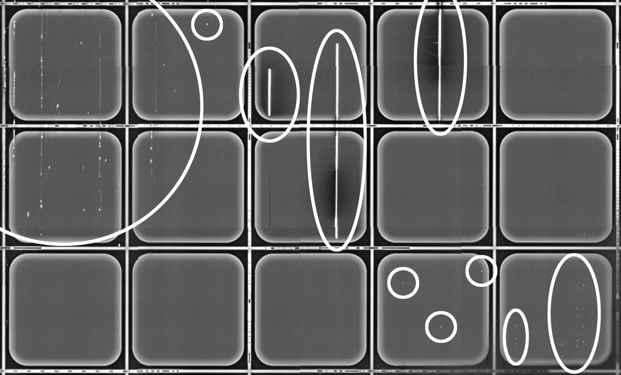
SiC is a demanding material when it comes to manufacture and processing. So far, the commercially available unipolar SiC devices have proved to be very reliable. On the other hand, bipolar SiC devices, which are needed for applications in energy systems with higher voltage classes, are still much more susceptible to certain material defects. These defects do not always cause an immediate failure, but may result in insidious degradation that, with today’s technology, can only be detected at great effort during manufacture or during the manufacturer’s final testing.
As part of the “SiC-WinS” project, the researchers at the Fraunhofer Institute for Integrated Systems and Device Technology IISB, together with their project partners, developed a cost-effective test that can be used to find the smallest defects on silicon carbide wafers – the raw material for innovative, particularly energy-efficient devices.
Measuring technology has room for improvement
Currently, an electrical stress test is used to detect degradation of SiC bipolar devices. Because this test is time-consuming and expensive, and cannot be used early in production at wafer level but can only be carried out on encapsulated devices, this method is not suitable for industrial production. The project partners’ idea was to measure the root cause of device degradation by means of direct mapping. For this reason, the researchers decided on the mapping photoluminescence (PL) method at room temperature in order to verify critical defects in industrial production lines. Until now, there has not been a PL measuring device that was fast enough to perform defect analysis on whole wafers, which would make it suitable for use in a production
Serial examination of SiC wafers
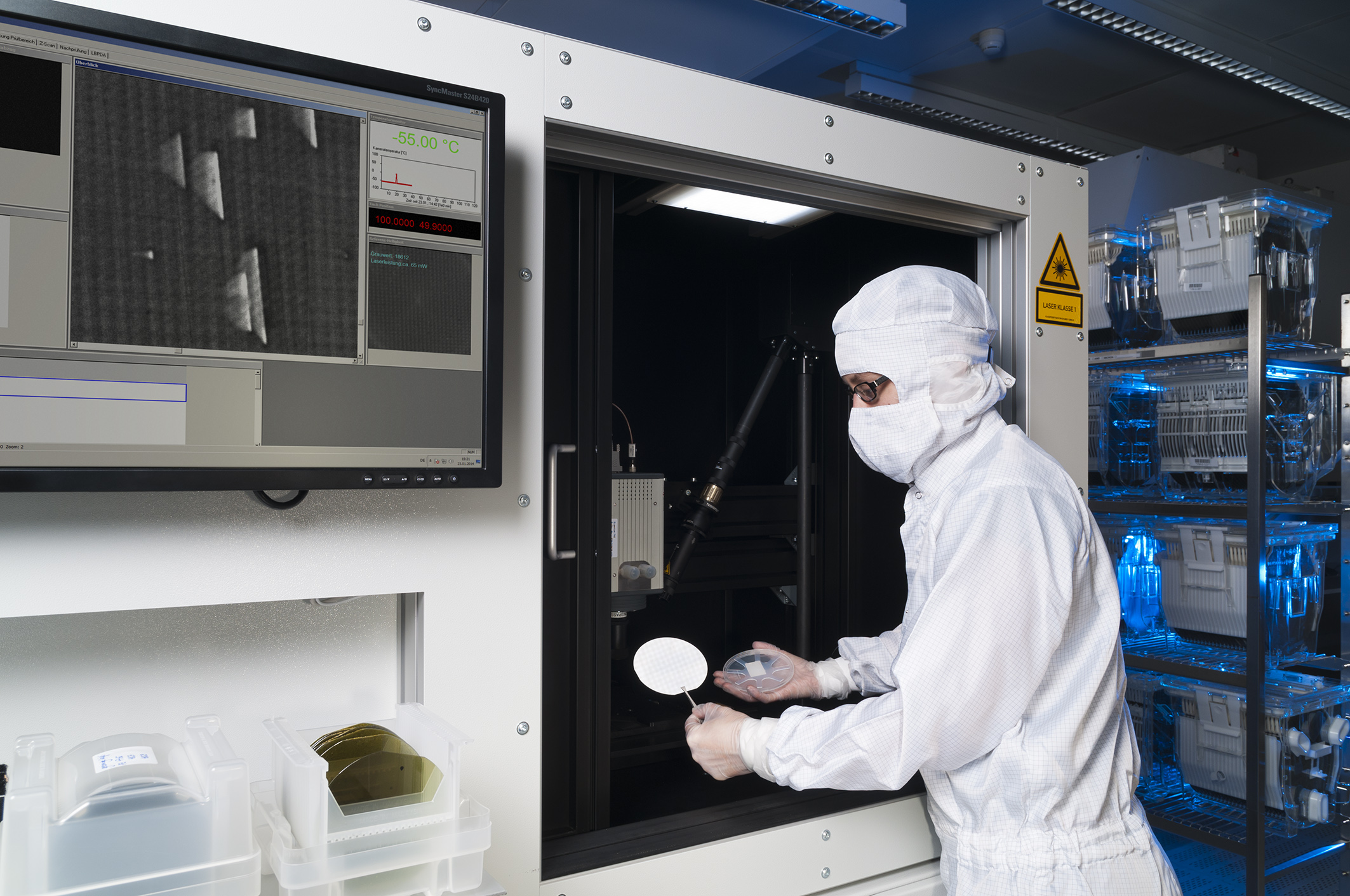
This challenge was met within the SiC-WinS project. A newly developed PL measuring device provides images of entire SiC wafers and all partially processed devices on it with a resolution of 2–5 μm. Critical devices that would fail later during operation can thus be identified with certainty and marked. The non-destructive and contactless measurement of a 150 mm wafer takes less than 30 minutes and can be repeated after different stages in the processing of the wafer. Already after the first process step in device production – epitaxial deposition of the drift area – the PL scanner identifies material defects in some of the as-yet unfinished devices. These are the devices that later fail during operation. This makes the newly developed inspection procedure an ideal complement to the quality control methods for the industrial production of bipolar SiC high-voltage devices. Thanks to its prediction of defective behavior, the PL measuring technology makes a direct contribution to the introduction of reliable and efficient bipolar SiC power devices in the energy and high-voltage market.
About the project:
In addition to Fraunhofer IISB, the following project partners are also involved: Infineon Technologies AG • Intego GmbH • Friedrich-Alexander- Universität Erlangen-Nürnberg. For the development of the innovative power electronics test, the project partners were presented with the SEMIKRON Innovation Award 2016. The SiC-WinS project was funded by the Bayerische Forschungsstiftung (Bavarian Research Foundation).
Last modified: