 Fraunhofer Group for Microelectronics
Structuring process for deep nanotrenches
Together with the Center for Microtechnologies (ZfM), Fraunhofer ENAS has developed a structuring process for silicon nano-trenches with a high aspect ratio.
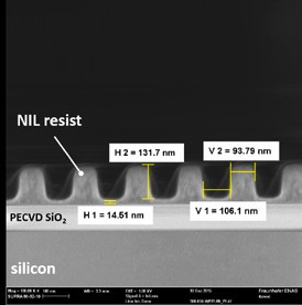
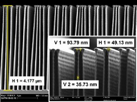
The aspect ratio refers to the relationship between the depth of the trench and its lateral extension. The deeper the trench, the higher its aspect ratio. The developed process flow allows the fabrication of trenches with a depth of more than 5 μm at a period of only 200 nm and an aspect ratio of more than 25:1.
New perspectives
Deep nano-trenches can be used to manufacture nano-meshes for X-ray Fabry-Perot interferometers for micro- and nano-electrical mechanical systems (known as MEMS or NEMS). The fabrication of piezo-resistive silicon nano-wires for inertial sensor technology or vertically arranged reactive multi-layer systems (v-RMS) for packaging is also conceivable.
The process
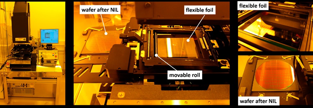
The manufacturing process includes several steps: first, chemical vapor deposition (PECVD) is applied to the surface of a silicon wafer in order to create a hard mask of silicon dioxide (SiO2). Subsequently, the nano- structures are transferred from a specially prepared foil into a viscous resist using the SmartNIL™ process (NIL: nano-imprint lithography). For preparation of nano-imprint lithography, the initial nanostructures are manufactured on a master wafer using electron-beam lithography and then transferred onto an elastic foil into a polymer. By applying a force to a movable roller, linear contact between the foil and the NIL resist is realized. The result is a significantly reduced defect rate. The resist is displaced by the polymer nanostructures, which forms a copy in the NIL lacquer. After etching the SiO2 hard mask, the silicon is deeply structured using deep reactive ion etching (DRIE).
Outlook
Especially for applications in the field of MEMS and NEMS technologies even higher process stability is necessary. True-to-size structure transfer with even lower tolerance deviations is at the forefront. There is also a plan to research the possibilities of extending the process to various metals.
Last modified: